The 3D-MAPS Processors
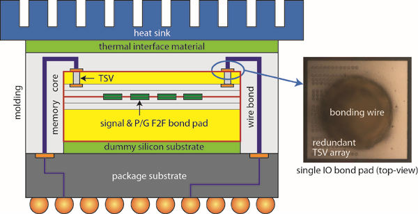
FIGURE 1: This is the stacking information of 3D-MAPS V1. We use bonding wires and TSVs for the package-to-chip signal and P/G delivery. Chip-to-chip communication is done using F2F pads. The bonding wires did not break the TSVs underneath during manufacturing. Each IO cell contains 204 redundant TSVs.
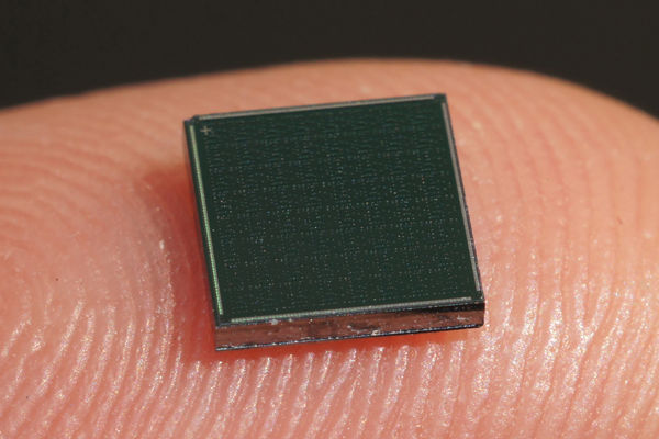
FIGURE 2: The topside of 3D-MAPS V1 is actually the backside of the core die that is thinned down to 12um. With bare eyes, we can only see dummy TSVs and IO cells.
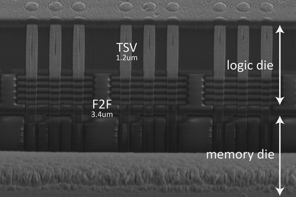
FIGURE 3: SEM image of Tezzaron TSVs and face-to-face bond pads.
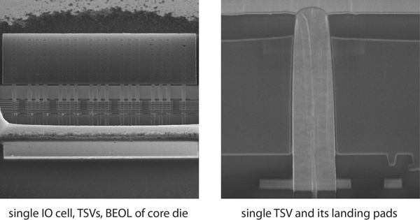
FIGURE 4: More SEM images of TSVs and F2F pads.
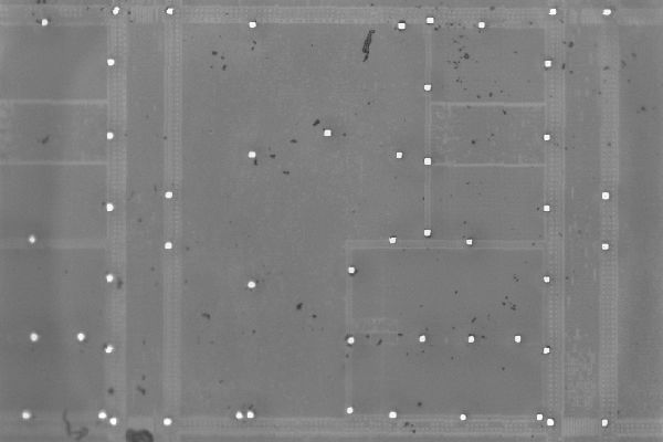
FIGURE 5: The above image is obtained using an infrared microscope with 6um depth. Since the top surface of 3D-MAPS V1 is the thinned substrate of top die, we had to use an IR microscope to reveal the circuitry that is buried under this substrate. The white dots are dummy TSVs we had to add to satisfy the TSV density rule set by Tezzaron.
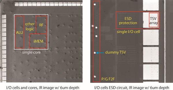
FIGURE 6: Some details of single core and single IO cell.
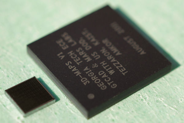
FIGURE 7: Bare die and its package side-by-side.
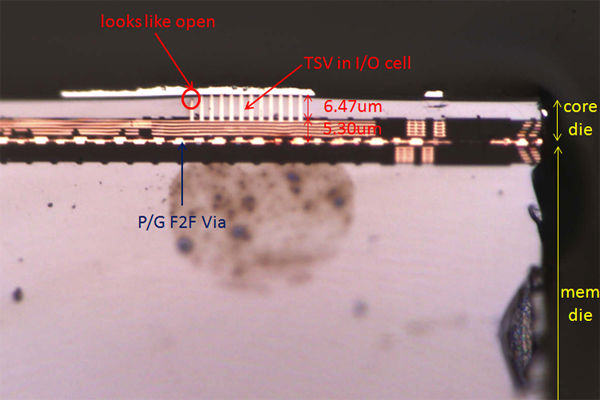
FIGURE 8: The open TSV above, fortunately, does not cause any problem because all of the TSVs shown are redundant. The top die (= core die) is thinned down to 12um, and the bottom die (= memory die) height is 765um, making the total thickness to be roughly 0.8mm.
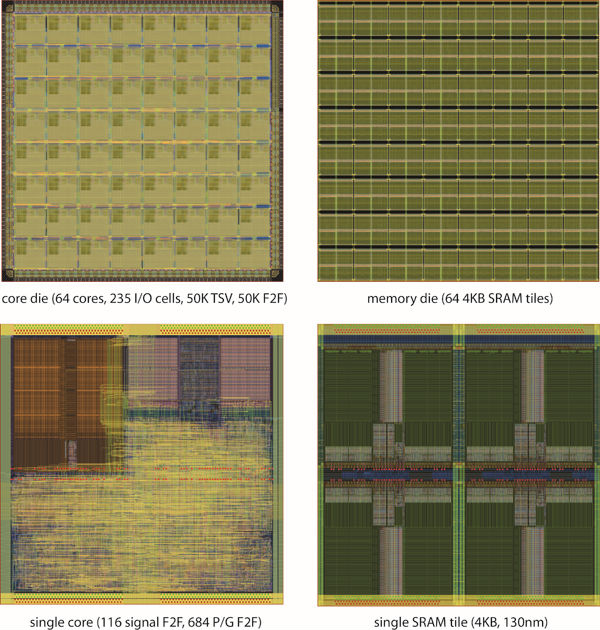
FIGURE 10: Layouts of full-die (core and memory) and single core/memory tile.
School of Electrical and Computer Engineering
Georgia Institute of Technology
777 Atlantic Drive NW
Atlanta, GA 30332-0250, USA
Office: KACB #2360
Phone: 404-894-0373
Email: limsk@ece.gatech.edu
http://users.ece.gatech.edu/limsk